-

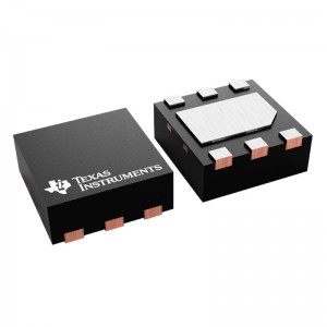
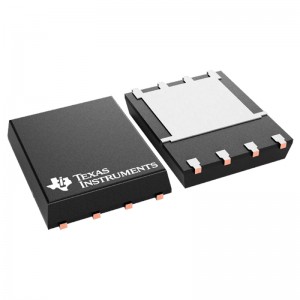
TPS259573DSGR WSON-8 Electronic components integrated circuit 2.7V-18V 4A
TPS259573DSGR 2.7-V to 18-V, 34mΩ, 0.5-4A eFuse with over voltage protection in small WSON package
The TPS2595xx family of eFuses (integrated FET hot swap devices) is a highly integratedcircuit protection and power management solution in a small package. The devices provide multipleprotection modes using very few external components and are a robust defense against overloads ,short circuits, voltage surges, and excessive inrush current.
Output current limit level can be set with a single external resistor. It is alsopossible to get an accurate sense of the output load current by measuring the voltage drop acrossthe current limit resistor. Applications with particular inrush current requirements can set theoutput slew rate with a single external capacitor. Overvoltage events are quickly limited byinternal clamping circuits to a safe fixed maximum, with no extermal components required. TheTPS259573 variant provides an option to set a user. defined overvoltage cutoff
threshold.
Quick output discharge function can be implemented in the TPS2595x5 variants byconnecting the OUT pin to the QOD pin.
The devices are characterized for operation over the temperature range of – 40°C to+ 125°C. -

TPS73533DRVR QFN-6 Electronic components integrated circuit 500mA Voltage regulator
TPS73533DRVR 500-mA, low-IQ, low-dropout voltage regulator with enable
The TPS735 low-dropout (LDO), low-power linear regulator offersexcellent AC performance with very low ground current. High power-supply rejection ratio (PSRR),low noise, fast start-up, and excellent line and load transient responses are provided whileconsuming a very low 45-µA (typical) ground current.
The TPS735 device is stable with ceramic capacitors and uses an advancedBiCMOS fabrication process to yield a typical dropout voltage of 280 mV at 500-mA output. TheTPS735 device uses a precision voltage reference and feedback loop to achieve overall accuracy of2% (VOUT > 2.2 V) over all load, line, process, and temperaturevariations. This device is fully specified from TJ = –40°C to +125°C and isoffered in a low-profile, 3 mm × 3 mm SON-8 package and a 2 mm × 2 mm WSON-6 package.
-

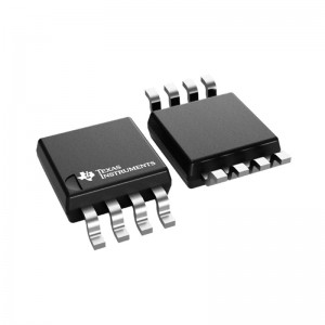
TLV272CDGKR MSOP-8 Electronic components integrated circuit 3MHz Amplifier chip
TLV272CDGKR Dual, 16-V, 3-MHz operational amplifier
Operating from 2.7 V to 16 V over the extended industrial temperature range from –40°C to +125°C, the TLV27x is a low power, wide bandwidth operational amplifier (opamp) with rail to rail output. This makes it an ideal alternative to the TLC27x family for applications where rail-to-rail output swings are essential. The TLV27x provides 3-MHz bandwidth from only 550 µA.
Like the TLC27x, the TLV27x is fully specified for 5-V and ±5-V supplies. The maximum recommended supply voltage is 16 V, which allows the devices to be operated from a variety of rechargeable cells (±8 V supplies down to ±1.35 V).
The CMOS inputs enable use in high-impedance sensor interfaces, with the lower voltage operation making an attractive alternative for the TLC27x in battery-powered applications.
All members are available in PDIP and SOIC with the singles in the small SOT-23 package, duals in the MSOP, and quads in the TSSOP package.
The 2.7-V operation makes it compatible with Li-Ion powered systems and the operating supply voltage range of many micropower microcontrollers available today including TI’s MSP430.
-

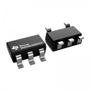
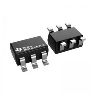
TPS7A2033PDBVR SOT-23-5 Electronic components integrated circuit Voltage regulator chip
TPS7A2033PDBVR
ACTIVE
300-mA, ultra-low-noise, low-IQ, low-dropout (LDO) linear regulator with high PSRRThe TPS7A20 is an ultra-small, low-dropout (LDO) linear regulator that can source 300 mA of output current. The TPS7A20 is designed to provide low noise, high PSRR, and excellent load and line transient performance that can meet the requirements of RF and other sensitive analog circuits. Using innovative design techniques, the TPS7A20 offers an ultra-low noise performance without the addition of a noise bypass capacitor. The TPS7A20 also provides the advantage of low quiescent current, which can be ideal for battery-powered applications. With an input voltage range of 1.6 V to 6.0 V and an output range of 0.8 V to 5.5 V, the TPS7A20 can be used for a wide variety of applications. The device uses a precision reference circuit to provide a maximum accuracy of 1.5% over load, line, and temperature variations.
The TPS7A20 features an internal soft-start to lower the inrush current, thus minimizing the input voltage drop during start up. The device is stable with small ceramic capacitors, allowing for a small overall solution size.
The TPS7A20 has a smart enable input circuit with an internally controlled pulldown resistor that keeps the LDO disabled even when the EN pin is left floating and helps eliminate the external components used to pulldown the EN pin.
-

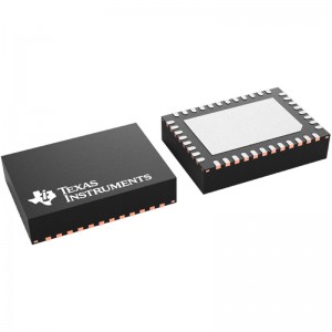
TPS548B22RVFR LQFN-40 Electronic components integrated circuit converter 1.5V-18V
TPS548B22RVFR 1.5-V to 18-V, 25-A synchronous SWIFT™ buck converter with differential remote sense
The TPS548B22 device is a compact single buck converter with adaptive on-time,D-CAP3 mode control. It is designed for high accuracy, high efficiency, fast transient response,ease-of-use, low external component count, and space-conscious power systems.
This device features full differential sense, TI integrated FETs with a high-sideon-resistance of 4.1 mΩ and a low-side on-resistance of 1.9 mΩ. The device alsofeatures accurate 0.5%, 0.9-V reference with an ambient temperature range between –40°C and +125°C.Competitive features include: very low external component count, accurate load regulation and lineregulation, output voltage setpoint accuracy, auto-skip or FCCM mode operation, and internalsoft-start control.
The TPS548B22device is available in 7 mm × 5 mm, 40-pin, LQFN-CLIP (RVF) package (RoHs exempt).
-

TPS73101DBVR SOT-23-5 Electronic components integrated circuit 1.7V-5.5V Voltage regulator
TPS73101DBVR 150-mA, high-accuracy, ultra-low-dropout voltage regulator with reverse current protection & enable
The TPS731xx family of low-dropout (LDO) linear voltage regulators uses a new topology: an NMOS pass element in a voltage-follower configuration. This topology is stable using output capacitors with low equivalent series resistance (ESR), and even allows operation without a capacitor. The device also provides high reverse blockage (low reverse current) and ground pin current that is nearly constant over all values of output current.
The TPS731xx uses an advanced BiCMOS process to yield high precision while delivering very low dropout voltages and low ground pin current. Current consumption, when not enabled, is less than 1 µA and ideal for portable applications. The extremely low output noise (30 µVRMS with 0.1-µF CNR) is ideal for powering VCOs. These devices are protected by thermal shutdown and foldback current limit.
-

TLV3202AIDGKR VSSOP8 Electronic components integrated circuit 1mV Validator IC
TLV3202AIDGKR
ACTIVE
5.5-V, high-speed, dual push-pull comparatorThe TLV3201 and TLV3202 are single- and dual-channel comparators that offer the ultimate combination of high speed (40 ns) and low-power consumption (40 µA), all in extremely small packages with features such as rail-to-rail inputs, low offset voltage (1 mV), and large output drive current. The devices are also very easy to implement in a wide variety of applications where response time is critical.
The TLV320x family is available in single (TLV3201) and dual (TLV3202) channel versions, both with push-pull outputs. The TLV3201 is available in 5-pin SOT-23 and 5-pin SC70 packages. The TLV3202 is available in 8-pin SOIC and 8-pin VSSOP packages. All devices are specified for operation across the expanded industrial temperature range of –40°C to 125°C.
-

LM324DR SOP-14 Electronic components integrated circuit amplifier 1.4mA 20nA
TLV3202AIDGKR
ACTIVE
5.5-V, high-speed, dual push-pull comparatorThe TLV3201 and TLV3202 are single- and dual-channel comparators that offer the ultimate combination of high speed (40 ns) and low-power consumption (40 μA), all in
extremely small packages with features such as rail-to-rail inputs, low offset voltage (1 mV), and large output drive current. The devices are also very easy to implement in a wide variety of applications where response time is critical.
The TLV320x family is available in single (TLV3201) and dual (TLV3202) channel versions, both with push-pull outputs. The TLV3201 is available in 5-pin SOT-23 and 5-pin SC70 packages. The TLV3202 is available in 8-pin SOIC and 8-pin VSSOP packages. All devices are specifed for operation across the expanded industrial temperature range of -
40°C to 125°C. -

CSD18531Q5A SON-8 Electronic components integrated circuit Separate semiconductor products
CSD18531Q5A 60-V, N channel NexFET™ power MOSFET, single SON 5 mm x 6 mm, 4.6 mOhm
This 60-V, 3.5-mΩ, 5-mm × 6-mm NexFET™ power MOSFETis designed to minimize losses in power conversionapplications.
-

TPS560430XDBVR SOT-23-6 Electronic components integrated circuit DC-DC Switching voltage stabilizer
TPS560430XDBVR SIMPLE SWITCHER® 36-V, 600-mA Buck Regulator With High-Efficiency Sleep Mode
The TPS560430 is an easy to use synchronous step-down DC-DC converter capable of drivingup to 600-mA load current. With a wide input range of 4 V to 36 V, the device is suitable for awide range of applications from industrial to automotive for power conditioning from an unregulatedsource.
The TPS560430 has 1.1-MHz and 2.1-MHz operating frequency versions for either highefficiency or small solution size. The TPS560430 also has FPWM (forced PWM) version to achieveconstant frequency and small output voltage ripple over the full load range. Soft-start andcompensation circuits are implemented internally which allows the device to be used with minimumexternal components.
The device has built-in protection features, such as cycle-by-cycle current limit, hiccupmode short-circuit protection, and thermal shutdown in case of excessive power dissipation. TheTPS560430 is available in SOT-23-6 package.
-

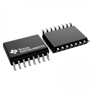
ISO7241CDWR SOP-16 Electronic components integrated circuit Digital isolator 3.15V-5.5V
ISO7241CDWR
ACTIVE
Quad-channel, 3/1, 25-Mbps digital isolatorThe ISO7240x, ISO7241x, and ISO7242x devices are quad-channel digital isolators withmultiple channel configurations and output-enable functions. These devices have logic-input andlogic-output buffers separated by Texas Instrument’s silicon-dioxide (SiO2)isolation barrier. Used in conjunction with isolated power supplies, these devices help block highvoltage, isolate grounds, and prevent noise currents from entering the local ground and interferingwith or damaging sensitive circuitry.
The ISO7240x family of devices has all four channels in the same direction. The ISO7241xfamily of devices has three channels in the same direction and one channel in the oppositiondirection. The ISO7242x family of devices has two channels in each direction.
The devices with the C suffix (C option) have TTL input thresholds and a noise-filter atthe input that prevents transient pulses from being passed to the output of the device. The deviceswith the M suffix (M option) have CMOS VCC/2 input thresholds and do nothave the input noise filter or the additional propagation delay.
The ISO7240CF device has an input disable function on pin 7, and a selectable high or lowfailsafe-output function with the CTRL pin (pin 10). The failsafe output is a logic high when alogic high is placed on the CTRL pin or it is left unconnected. If a logic low signal is applied tothe CTRL pin, the failsafe output becomes a logic-low output state. The input disable function ofthe ISO7240CF device prevents data from being passed across the isolation barrier to the output.When the inputs are disabled or VCC1 is powered down, the outputs are set bythe CTRL pin.
These devices can be powered from 3.3-V or 5-V supplies on either side, in anycombination. The signal input pins are 5-V tolerant regardless of the voltage supply level that isused.
These devices are characterized for operation over the ambient temperature range of –40°Cto +125°C.
-

SN75LBC176DR SOP-8 Electronic components integrated circuit transceiver 4.75V-5.25V
SN75LBC176DR Differential Bus Transceiver
The SN55LBC176, SN65LBC176, SN65LBC176Q, and SN75LBC176 differential bus transceivers are monolithic, integrated circuits designed for bidirectional data communication on multipoint bus-transmission lines. They are designed for balanced transmission lines and meet ANSI Standard TIA/EIA-485-A (RS-485) and ISO 8482:1987(E).
The SN55LBC176, SN65LBC176, SN65LBC176Q, and SN75LBC176 combine a 3-state, differential line driver and a differential input line receiver, both of which operate from a single 5-V power supply. The driver and receiver have active-high and active-low enables, respectively, which can externally connect together to function as a direction control. The driver differential outputs and the receiver differential inputs connect internally to form a differential input/output (I/O) bus port that is designed to offer minimum loading to the bus whenever the driver is disabled or VCC = 0. This port features wide positive and negative common-mode voltage ranges, making the device suitable for party-line applications. Very low device supply current can be achieved by disabling the driver and the receiver.


